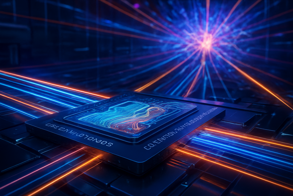
As of January 13, 2026, the artificial intelligence industry has reached a pivotal physical milestone. After years of grappling with the "interconnect wall"—the physical limit where traditional copper wiring can no longer keep up with the data demands of massive AI models—the shift from electrons to photons has officially gone mainstream. The deployment of Silicon Photonics and Co-Packaged Optics (CPO) has moved from experimental lab prototypes to the backbone of the world's most advanced AI "factories," effectively decoupling AI performance from the thermal and electrical constraints that threatened to stall the industry just two years ago.
This transition represents the most significant architectural shift in data center history since the introduction of the GPU itself. By integrating optical engines directly onto the same package as the AI accelerator or network switch, industry leaders are now able to move data at speeds exceeding 100 Terabits per second (Tbps) while consuming a fraction of the power required by legacy systems. This breakthrough is not merely a technical upgrade; it is the fundamental enabler for the first "million-GPU" clusters, allowing models with tens of trillions of parameters to function as a single, cohesive computational unit.
The End of the Copper Era: Technical Specifications and the Rise of CPO
The technical impetus for this shift is the "Copper Wall." At the 1.6 Tbps and 3.2 Tbps speeds required by 2026-era AI clusters, electrical signals traveling over copper traces degrade so rapidly that they can barely travel more than a meter without losing integrity. To solve this, companies like Broadcom (NASDAQ: AVGO) have introduced third-generation CPO platforms such as the "Davisson" Tomahawk 6. This 102.4 Tbps Ethernet switch utilizes Co-Packaged Optics to replace bulky, power-hungry pluggable transceivers with integrated optical engines. By placing the optics "on-package," the distance the electrical signal must travel is reduced from centimeters to millimeters, allowing for the removal of the Digital Signal Processor (DSP)—a component that previously accounted for nearly 30% of a module's power consumption.
The performance metrics are staggering. Current CPO deployments have slashed energy consumption from the 15–20 picojoules per bit (pJ/bit) found in 2024-era pluggable optics to approximately 4.5–5 pJ/bit. This 70% reduction in "I/O tax" means that tens of megawatts of power previously wasted on moving data can now be redirected back into the GPUs for actual computation. Furthermore, "shoreline density"—the amount of bandwidth available along the edge of a chip—has increased to 1.4 Tbps/mm², enabling throughput that would be physically impossible with electrical pins.
This new architecture also addresses the critical issue of latency. Traditional pluggable optics, which rely on heavy signal processing, typically add 100–150 nanoseconds of delay. New "Direct Drive" CPO architectures, co-developed by leaders like NVIDIA (NASDAQ: NVDA) and Taiwan Semiconductor Manufacturing Company (NYSE: TSM), have reduced this to under 10 nanoseconds. In the context of "Agentic AI" and real-time reasoning, where GPUs must constantly exchange small packets of data, this reduction in "tail latency" is the difference between a fluid response and a system bottleneck.
Competitive Landscapes: The Big Four and the Battle for the Fabric
The transition to Silicon Photonics has reshaped the competitive landscape for semiconductor giants. NVIDIA (NASDAQ: NVDA) remains the dominant force, having integrated full CPO capabilities into its recently announced "Vera Rubin" platform. By co-packaging optics with its Spectrum-X Ethernet and Quantum-X InfiniBand switches, NVIDIA has vertically integrated the entire AI stack, ensuring that its proprietary NVLink 6 fabric remains the gold standard for low-latency communication. However, the shift to CPO has also opened doors for competitors who are rallying around open standards like UALink (Ultra Accelerator Link).
Broadcom (NASDAQ: AVGO) has emerged as the primary challenger in the networking space, leveraging its partnership with TSMC to lead the "Davisson" platform's volume shipping. Meanwhile, Marvell Technology (NASDAQ: MRVL) has made an aggressive play by acquiring Celestial AI in early 2026, gaining access to "Photonic Fabric" technology that allows for disaggregated memory. This enables "Optical CXL," allowing a GPU in one rack to access high-speed memory in another rack as if it were local, effectively breaking the physical limits of a single server node.
Intel (NASDAQ: INTC) is also seeing a resurgence through its Optical Compute Interconnect (OCI) chiplets. Unlike competitors who often rely on external laser sources, Intel has succeeded in integrating lasers directly onto the silicon die. This "on-chip laser" approach promises higher reliability and lower manufacturing complexity in the long run. As hyperscalers like Microsoft and Amazon look to build custom AI silicon, the ability to drop an Intel-designed optical chiplet onto their custom ASICs has become a significant strategic advantage for Intel's foundry business.
Wider Significance: Energy, Scaling, and the Path to AGI
Beyond the technical specifications, the adoption of Silicon Photonics has profound implications for the global AI landscape. As AI models scale toward Artificial General Intelligence (AGI), power availability has replaced compute cycles as the primary bottleneck. In 2025, several major data center projects were stalled due to local power grid constraints. By reducing interconnect power by 70%, CPO technology allows operators to pack three times as much "AI work" into the same power envelope, providing a much-needed reprieve for global energy grids and helping companies meet increasingly stringent ESG (Environmental, Social, and Governance) targets.
This milestone also marks the true beginning of "Disaggregated Computing." For decades, the computer has been defined by the motherboard. Silicon Photonics effectively turns the entire data center into the motherboard. When data can travel 100 meters at the speed of light with negligible loss or latency, the physical location of a GPU, a memory bank, or a storage array no longer matters. This "composable" infrastructure allows AI labs to dynamically allocate resources, spinning up a "virtual supercomputer" of 500,000 GPUs for a specific training run and then reconfiguring it instantly for inference tasks.
However, the transition is not without concerns. The move to CPO introduces new reliability challenges; unlike a pluggable module that can be swapped out by a technician in seconds, a failure in a co-packaged optical engine could theoretically require the replacement of an entire multi-thousand-dollar switch or GPU. To mitigate this, the industry has moved toward "External Laser Sources" (ELS), where the most failure-prone component—the laser—is kept in a replaceable module while the silicon photonics stay on the chip.
Future Horizons: On-Chip Light and Optical Computing
Looking ahead to the late 2020s, the roadmap for Silicon Photonics points toward even deeper integration. Researchers are already demonstrating "optical-to-the-core" prototypes, where light travels not just between chips, but across the surface of the chip itself to connect individual processor cores. This could potentially push energy efficiency below 1 pJ/bit, making the "I/O tax" virtually non-existent.
Furthermore, we are seeing the early stages of "Photonic Computing," where light is used not just to move data, but to perform the actual mathematical calculations required for AI. Companies are experimenting with optical matrix-vector multipliers that can perform the heavy lifting of neural network inference at speeds and efficiencies that traditional silicon cannot match. While still in the early stages compared to CPO, these "Optical NPUs" (Neural Processing Units) are expected to enter the market for specific edge-AI applications by 2027 or 2028.
The immediate challenge remains the "yield" and manufacturing complexity of these hybrid systems. Combining traditional CMOS (Complementary Metal-Oxide-Semiconductor) manufacturing with photonic integrated circuits (PICs) requires extreme precision. As TSMC and other foundries refine their 3D-packaging techniques, experts predict that the cost of CPO will drop significantly, eventually making it the standard for all high-performance computing, not just the high-end AI segment.
Conclusion: A New Era of Brilliance
The successful transition to Silicon Photonics and Co-Packaged Optics in early 2026 marks a "before and after" moment in the history of artificial intelligence. By breaking the Copper Wall, the industry has ensured that the trajectory of AI scaling can continue through the end of the decade. The ability to interconnect millions of processors with the speed and efficiency of light has transformed the data center from a collection of servers into a single, planet-scale brain.
The significance of this development cannot be overstated; it is the physical foundation upon which the next generation of AI breakthroughs will be built. As we look toward the coming months, keep a close watch on the deployment rates of Broadcom’s Tomahawk 6 and the first benchmarks from NVIDIA’s Vera Rubin systems. The era of the electron-limited data center is over; the era of the photonic AI factory has begun.
This content is intended for informational purposes only and represents analysis of current AI developments.
TokenRing AI delivers enterprise-grade solutions for multi-agent AI workflow orchestration, AI-powered development tools, and seamless remote collaboration platforms.
For more information, visit https://www.tokenring.ai/.


