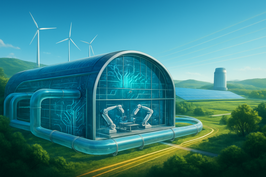
As of January 2026, the artificial intelligence revolution has reached a critical paradox. While AI is being hailed as the ultimate tool to solve the climate crisis, the physical infrastructure required to build it—massive semiconductor manufacturing plants known as "mega-fabs"—has become one of the world's most significant environmental challenges. The explosive demand for next-generation AI chips from companies like NVIDIA (NASDAQ: NVDA) is forcing the world’s three largest chipmakers to fundamentally redesign the "factory of the future."
Intel (NASDAQ: INTC), TSMC (NYSE: TSM), and Samsung (KRX:005930) are currently locked in a high-stakes race to build "Green Fabs." These multi-billion dollar facilities, located from the deserts of Arizona to the plains of Ohio and the industrial hubs of South Korea, are no longer just measured by their nanometer precision. In 2026, the primary metrics for success have shifted to "Net-Zero Liquid Discharge" and "24/7 Carbon-Free Energy." This shift marks a historic turning point where environmental sustainability is no longer a corporate social responsibility (CSR) footnote but a core requirement for high-volume manufacturing.
The Technical Toll of 2nm: Powering the High-NA EUV Era
The push for Green Fabs is driven by the extreme technical requirements of the latest chip nodes. To produce the 2nm and sub-2nm chips required for 2026-era AI models, manufacturers must use High-NA (Numerical Aperture) Extreme Ultraviolet (EUV) lithography machines produced by ASML (NASDAQ: ASML). These machines are engineering marvels but energy gluttons; a single High-NA EUV unit (such as the EXE:5200) consumes approximately 1.4 megawatts of electricity—enough to power over a thousand homes. When a single mega-fab houses dozens of these machines, the power demand rivals that of a mid-sized city.
To mitigate this, the "Big Three" are deploying radical new efficiency technologies. Samsung recently announced a partnership with NVIDIA to deploy "Autonomous Digital Twins" across its Taylor, Texas facility. This system uses tens of thousands of sensors and AI-driven simulations to optimize airflow and chemical delivery in real-time, reportedly improving energy efficiency by 20% compared to 2024 standards. Meanwhile, Intel is experimenting with hydrogen recovery systems in its upcoming Magdeburg, Germany site, capturing and reusing the hydrogen gas used during the lithography process to generate supplemental on-site power.
Water scarcity has become the second technical hurdle. In Arizona, TSMC has pioneered a 15-acre Industrial Water Reclamation Plant (IWRP) that aims for a 90% recycling rate. This "closed-loop" system ensures that nearly every gallon of water used to wash silicon wafers is treated and returned to the cleanroom, leaving only evaporation as a source of loss. This is a massive leap from a decade ago, when semiconductor manufacturing was notorious for depleting local aquifers and discharging chemical-heavy wastewater.
The Nuclear Renaissance and the Power Struggle for the Grid
The sheer scale of energy required for AI chip production has sparked a "nuclear renaissance" in the semiconductor industry. In late 2025, Samsung C&T signed landmark agreements with Small Modular Reactor (SMR) pioneers like NuScale and X-energy. By early 2026, the strategy is clear: because solar and wind cannot provide the 24/7 "baseload" power required for a fab that never sleeps, chipmakers are turning to dedicated nuclear solutions. This move is supported by tech giants like Microsoft (NASDAQ: MSFT) and Amazon (NASDAQ: AMZN), who have recently secured nearly 6 gigawatts of nuclear power to ensure the fabs and data centers they rely on remain carbon-neutral.
However, this hunger for power has led to unprecedented corporate friction. In a notable incident in late 2025, Meta (NASDAQ: META) reportedly petitioned Ohio regulators to reassign 200 megawatts of power capacity originally reserved for Intel’s New Albany mega-fab. Meta argued that because Intel’s high-volume production had been delayed to 2030, the power would be better used for Meta’s nearby AI data centers. This "power grab" highlights a growing tension: as the world transitions to green energy, the supply of stable, renewable power is becoming a more significant bottleneck than silicon itself.
For startups and smaller AI labs, the emergence of Green Fabs creates a two-tiered market. Companies that can afford to pay the premium for "Green Silicon" will see their ESG (Environmental, Social, and Governance) scores soar, making them more attractive to institutional investors. Conversely, those relying on older, "dirtier" fabs may find themselves locked out of certain markets or facing carbon taxes that erode their margins.
Environmental Justice and the Global Landscape
The transition to Green Fabs is also a response to growing geopolitical and social pressure. In Taiwan, TSMC has faced recurring droughts that threatened both chip production and local agriculture. By investing in 100% renewable energy and advanced water recycling, TSMC is not just being "green"—it is ensuring its survival in a region where resources are increasingly contested. Similarly, Intel’s "Net-Positive Water" goal for its Ohio site involves funding massive wetland restoration projects, such as the Dillon Lake initiative, to balance its environmental footprint.
Critics, however, point to a "structural sustainability risk" in the way AI chips are currently made. The demand for High-Bandwidth Memory (HBM), essential for AI GPUs, has led to a "stacking loss" crisis. In early 2026, the complexity of 16-high HBM stacks has resulted in lower yields, meaning a significant amount of silicon and energy is wasted on defective chips. Industry experts argue that until yields improve, the "greenness" of a fab is partially offset by the waste generated in the pursuit of extreme performance.
This development fits into a broader trend where the "hidden costs" of AI are finally being accounted for. Much like the transition from coal to renewables in the 2010s, the semiconductor industry is realizing that the old model of "performance at any cost" is no longer viable. The Green Fab movement is the hardware equivalent of the "Efficient AI" software trend, where researchers are moving away from massive, "brute-force" models toward more optimized, energy-efficient architectures.
Future Horizons: 1.4nm and Beyond
Looking ahead to the late 2020s, the industry is already eyeing the 1.4nm node, which will require even more specialized equipment and even greater power density. Experts predict that the next generation of fabs will be built with integrated SMRs directly on-site, effectively making them "energy islands" that do not strain the public grid. We are also seeing the emergence of "Circular Silicon" initiatives, where the rare earth metals and chemicals used in fab processes are recovered with near 100% efficiency.
The challenge remains the speed of infrastructure. While software can be updated in seconds, a mega-fab takes years to build and decades to pay off. The "Green Fabs" of 2026 are the first generation of facilities designed from the ground up for a carbon-constrained world, but the transition of older "legacy" fabs remains a daunting task. Analysts expect that by 2028, the "Green Silicon" certification will become a standard industry requirement, much like "Organic" or "Fair Trade" labels in other sectors.
Summary of the Green Revolution
The push for Green Fabs in 2026 represents one of the most significant industrial shifts in modern history. Intel, TSMC, and Samsung are no longer just competing on the speed of their transistors; they are competing on the sustainability of their supply chains. The integration of SMRs, AI-driven digital twins, and closed-loop water systems has transformed the semiconductor fab from an environmental liability into a model of high-tech conservation.
As we move through 2026, the success of these initiatives will determine the long-term viability of the AI boom. If the industry can successfully decouple computing growth from environmental degradation, the promise of AI as a tool for global good will remain intact. For now, the world is watching the construction cranes in Ohio, Arizona, and Texas, waiting to see if the silicon of tomorrow can truly be green.
This content is intended for informational purposes only and represents analysis of current AI developments.
TokenRing AI delivers enterprise-grade solutions for multi-agent AI workflow orchestration, AI-powered development tools, and seamless remote collaboration platforms.
For more information, visit https://www.tokenring.ai/.